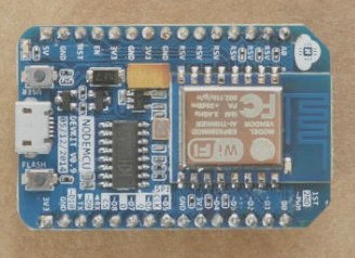
A friend from work let me borrow an ESP8266 module on a NodeMCU board and I went about trying to get started with it and thought I’d write up my notes. (using C++)
To make this easier I’m going to use the easily available Arduino IDE and a set of libraries for the ESP8266 module.
Using these libraries you can follow the steps below to enable your Arduino IDE to work with many ESP8266 modules. https://github.com/esp8266/Arduino
Using the Arduino IDE Boards Manager:
Start Arduino and open Preferences window.
Enter http://arduino.esp8266.com/stable/package_esp8266com_index.json into Additional Board Manager URLs field. You can add multiple URLs, separating them with commas.
Open Boards Manager from Tools > Board menu and install esp8266 platform.
Select your ESP8266 board from Tools > Board menu.
Code for the ESP8266 server
#include <ESP8266WiFi.h>
#include <WiFiClient.h>
#include <ESP8266WebServer.h>
#include <ESP8266mDNS.h>

const char* ssid = "YourWifiName";
const char* password = "YourWifiPassword";

void HandleRoot();
void HandleCommand();
void FlashLeds();
void TurnOffLeds();
void HandleNotFound();


ESP8266WebServer server(80);

// what to do when a client requests "http://<IP>"
void HandleRoot() {
    server.send(200, "text/plain", "hello from esp8266!");
}

// What to do when a client requests "http://<IP>/command"
// This function doesn't care whether it is a GET or POST at the moment,
// it will treat them the same just to make things easier.
void HandleCommand() {
    for (uint8_t i=0; i<server.args(); i++) {
        if (server.argName(i) == "flash") {
            if (server.arg(i) == "on") {
                FlashLeds();
                server.send(200, "text/plain", "LEDs turned on");
            } else {
                TurnOffLeds();
                server.send(200, "text/plain", "LEDs turned off");
            }
        }
    }
    server.send(404, "text/plain", "Command not found");
}

void FlashLeds() {
    // Flash LEDs or something then exit this func so that the webserver carries on running.
    Serial.println("LEDs on.");
}

void TurnOffLeds() {
    // Flash LEDs or something then exit this func so that the webserver carries on running.
    Serial.println("LEDs off.");
}

// If the route is not found then default to printing out what was sent to this server to aid in debug.
void HandleNotFound() {
    String message = "File Not Found\n\n";
    message += "URI: ";
    message += server.uri();
    message += "\nMethod: ";
    message += (server.method() == HTTP_GET)?"GET":"POST";
    message += "\nArguments: ";
    message += server.args();
    message += "\n";
    for (uint8_t i=0; i<server.args(); i++) {
        message += " " + server.argName(i) + ": " + server.arg(i) + "\n";
    }
    server.send(404, "text/plain", message);}

void setup(void) {
    Serial.begin(115200);
    WiFi.begin(ssid, password);
    Serial.println("Setting up.");

    // Wait for connection
    while (WiFi.status() != WL_CONNECTED) {
        delay(500);
        Serial.print(".");
    }
    Serial.println(".");
    Serial.print("Connected to ");
    Serial.println(ssid);
    Serial.print("IP address: ");
    Serial.println(WiFi.localIP());

    if (MDNS.begin("esp8266")) {
        Serial.println("MDNS responder started");
    }

    /*
    //I left this in commented out just to show this method as well.
    server.on("/inline", []() {
        server.send(200, "text/plain", "this works as well");
    });
    */

    // Setup server routes.
    server.on("/", HandleRoot);
    server.on("/command", HandleCommand);
    server.onNotFound(HandleNotFound);
    server.begin();
    Serial.println("HTTP server started");
}

void loop(void) {
    server.handleClient();
}
Code for webpage to send commands
The below code can be copied and pasted into a text file and then save the file as yourfilename.html, it will allow you to send commands to the module / server.
The IP address of my module is 192.168.1.115 so make sure you replace that IP in the below code with the one of your module.
Also note that you could actually serve this page straight from the module itself and not have separate file.
<head>
    <!--<script src="jquery.js"></script>-->
    <script src="http://code.jquery.com/jquery-2.2.1.min.js "></script>

 <script>
    $(function () {

    // Bind the click of the button to the function that posts data to the server.
    $('#buttonFlashOn').click( function() {
        $.post("http://192.168.1.115/command", { flash : "on"})
         .done(function( data ) {
             //alert( "Data returned: " + data );
        });
    });

    // bind the click of the button to the function that posts data to the server.
    $('#buttonFlashOff').click( function() {
        $.post("http://192.168.1.115/command", { flash : "off"})
         .done(function( data ) {
            //alert( "Data returned: " + data );
          });
    });

});
</script>


</head>

<body>
 <br/>
 <button id="buttonFlashOn">Flash on</button>
 <br/>
 <br/>
 <button id="buttonFlashOff">Flash off</button>
 <br/>
</body>
Within this article the author John ( G8GKU ) indicates how two typical AD9850 modules may be utilized and controlled so as to produce the often needed pair of R.F. carriers with a quadrature phase relationship, sine or cos (0° or 90°). These modules are readily available from online suppliers.
A pair of quadrature related sine waves are useful if not mandatory when making SSB modulators / demodulators, image reject mixers, Weaver method SSB ( Tx / Rx ) and similar items.
An accompanying demonstration code has been written to allow a user to set output frequency and phase of the two DDS units.
The popular Arduino™ platform has been chosen as controller for the DDS synthesisers, C++ Arduino code being written by Alex. However, to broaden the appeal, a version has also been coded which will run on a PIC™ 16F876 28 pin DIP device, written by G8GKU, providing home-brew readers an opportunity to warm up the soldering iron and build a system from scratch.
Download of the necessary hex file for the PIC 16F876 is available : Hex_Files
… and the Arduino equivalent is available here: dds
The author wishes to acknowledge, with thanks, the detailed technical information contained within the two publications by Analog Devices.
Photograph 1 shows the pair of DDS modules used by the author, however, there are other schematically similar but physically different PCBs to be obtained, the on-board circuitry is very similar and readers may well use their own choice of DDS module.
Photograph 1:
Overall the process consists of two parts:
Part one details the hardware implementation.
Part two introduces the procedure required to drive the physical DDS cores to produce the quadrature output waveforms.
Hardware Implementation
One small change is required to just one of the two DDS PCBs. The two DDS units are then physically mounted such that the DDS modules are close together, in a position which will allow the high speed crystal clock signal from one unit to be jumper-wired across to the second unit.
To allow the generation of frequency and phase locked quadrature outputs it is essential that both DDS modules share just one clock oscillator.
Note, Photograph 1 shows the M3 mounting screw-head adjacent to the double row of PCB connector pins, with the inside edge of the screw head filed back 1 mm. This is suggested as the DDS PCB has a signal track rather close to the hole. It is under the white indent paint and can easily be overlooked. Do this, at one position, for both DDS PCBs.
Photograph 1 indicates how the two DDS modules should be mounted, side by side and long-ways reversed, with ca 5.5 mm lengthways offset between them. This mounting method will allow the 125 MHz clock from one module to be passed across to the second module via a short wire, so keeping the two DDS clock signals closely in step as per the AN-587.pdf application note. Also visible is the strongly suggested addition of a short length of single sided PCB material, resulting in an overall mechanically firm assembly.
Required physical modification of DDS PCB.
It is required to modify just one of the DDS PCB modules, plus an extra option as mentioned below. In overview, one resistor is to lifted up on end and then a wire link added using as short a length of wire as is possible. Please view the wiring schematic sheet at this stage.
Method
Re photograph 1, the resistor to be lifted is indicated by the adjacent ink mark line on the joining PCB. This is a 100 Ohm resistor fitted between the xtal clock oscillator signal output ( pin 3 ) and the clock input to the AD9850 chip itself. The resistor and local circuitry is shown in very simplified fashion within the wiring diagram.
Choose one module on which the resistor is to be lifted to the vertical, on this DDS PCB the clock oscillator is then unused.
Using a small soldering iron, heat the soldered resistor pads by swapping end to end and lift it off the PCB with small tweezers, putting it in a safe place! Note, apply enough heat to not only melt the solder but also perhaps to melt the mounting glue used to affix the resistor before it was originally soldered.
Once the resistor is removed, ensure the then exposed PCB pads are free of solder spikes, perhaps applying a little new solder to the one vacated solder pad which is the inside-most pad, i.e. far-most from the PCB edge.
Refit the resistor so as to be vertical, on the inside pad, soldering one end to the pad. This so-called ‘ Tombstone ‘ fitting of the resistor is not strong and appropriate care is now needed when handling the PCB.
Consider the optional modification as below and then proceed to assemble the two PCBs side by as in photograph 2.
Photograph 2:
An Optional Modification
Optionally, the now unused clock oscillator module upon the DDS PCB which has been modified may be disabled, i.e. turned off. This has the advantage of saving the 40 mA or so of oscillator power supply demand and also removing the presence of an un-needed 125 MHz carrier which may be detected by nearby suitable Rx’s. To disable the oscillator module, proceed as follows :
Locate the oscillator module, it is the 7 x 5 mm metal clad component near the board edge.
Next locate pin 1 of the crystal module, it is the pin which is closest to both the board edge and the nearest PCB mounting hole. It is adjacent to the ‘ dot ‘ on the oscillator top cover. Clean off the paint from a 2 mm section of the PCB ground track just adjacent to pin 1 of the oscillator, there is a thin continuous ground track which runs past the module. Solder a 1.5 mm link, using thin wire, between the pin 1 pad of the oscillator and the cleaned PCB ground track. Job done.
Assembling the Two DDS Units
This section addresses assembling the two DDS units to be one module.
To provide workable physical strength a short strip of single sided copper clad PCB material is used to join two DDS PCBs, this may be glass fibre ( fiber ) PCB or other material. Suggested size of the material is 46 mm long by 11 mm wide. Two holes along each long edge are required, which are easiest to mark with a felt tip pen through the fixing holes of the DDS modules.
Mark holes on to the glass side and not the copper side of the strip. Photograph 1 shows the general technique.
Repeated from above ;
Please note, viewing Photograph 1 shows the M3 screw-head adjacent to the double row of PCB connector pins to have the inside edge of the screw head filled back 1 mm, this is needed as the DDS PCB has a signal track rather too close to the hole. It is under the indent paint and can easily be overlooked. Do this for both DDS PCBs.
The assembly is completed by bonding the pair of DDS PCBs together with the PCB joining material by use of either M3 or other slim nuts and bolts. Ensure that the joining plate has the copper side *away* from the DDS PCBs when assembling, take care not to allow a screwdriver to slip during this process, as it may damage surface mount components of the DDS modules.
These 4 non-insulated screws provide, via the PCB material, an additional overall ground connection between the two DDS modules. To allow the combined dual DDS assembly to stand on the bench for testing the author has fitted longer M3 screws to the four outside fixing holes to act as legs, nothing more.
Before fitting the clock signal wire link, carefully clean off the ground-track paint from a 3 mm length of the track, at both PCB edges just between the two 100 Ohm resistors. Once clean add a small ( about 2 mm ) bridging solder blob so as to join the ground tracks. This can be seen on photograph 2 ( it may be easier to remove the paint before final physical assembly ).
The wire link for the clock signal is next to be fitted. It should be taken from the non-modified DDS PCB, from the *outside* pad of the corresponding resistor which was lifted on the other PCB. The destination of the wire link is the top, i.e. free end, of the uplifted 100 Ohm resistor.
Use of thin enameled wire will reduce risk of unwanted connections, the wire link is about 7 mm long.
Physical Wiring
The diagram above shows the detailed pin to pin data signal wiring between the controller and the DDS module. However, please read the following application note.
Application note AN587 places strong emphasis upon the need for both the master clock to the DDS modules and the Frequency Update ( Fr_updt ) pulse to be applied with the same time, phase, relationship to each DDS in the system.
In particular the Fr_updt pulse should be a fast rising edge and should have the same physical wire length between the CPU / controller pin and to each DDS unit. It is *not correct* to daisy chain the Fr_updt pulse from the controller to a first DDS and then to pass it along to the second unit. The correct method is to fork, i.e. to split, the wire a little way before the wire reaches either one of the DDS units and to take one each of the forked wires to a DDS Fr_updt pin, keeping the wire lengths after the fork to closely the same length. This method will provide a Fr_updt pulse well time-matched to each DDS core. Likewise, the link-jumpered master clock signal will also be as close to in-phase as can be practically done by the close physical assembly of the two DDS units.
Part two introduces the code and operating procedure required to drive the physical units.
There is little in the code which will not be found in just about any code which drives an AD9850 module. What makes the code for this article different is that it sequences the start up of the two DDS cores in the correct fashion so as to run not only at the same frequency but with a quadrature phase relationship.
The DDS start-up sequence in this article refers to the DDS units as operated in the serial mode of data loading, the parallel mode is only slightly different.
Overall the process consists of clearing all of the registers of the two DDS units and then starting both, at the required frequency and phase angle with a single “ go “ pulse from the controller. However, the AD9850 has some subtle characteristics which are important to the start up process.
Although contained within the data sheet, what is quite easily overlooked is the information that the AD9850 device always starts-up in parallel data entry mode at any reset pulse application.
Added to this situation is that the very first ‘ data-load clock pulse, Fr_updt pulse pair ‘ ( in that order ) following a reset always has the task of loading the internal 8 bit control and phase register of the AD9850, keep in mind this is an 8 bit parallel load event. In this application, it is required that the AD9850 starts at “ zero phase “ or some other selectable phase. Therefore the relevant bits of the phase control word must be pre-set, at the very first ‘data-load clock pulse Fr_updt pulse pair’. The solution used in this article is to ensure the phase control bits are held, wired, at logic 0 during the first data-load clock pulse, Fr_updt pulse pair. It is then the responsibility of the second update pulse to load the actual required phase and frequency data. To ensure the initial phase select bits are at logic zero, in the case of the DDS module used by the author, the data pins, D3, 4, 5, 6 are wire linked to zero volts, i.e. the ground pin of the connector. Data bits 0, 1 are set to logic 1 by on-PCB pull up resistors and a two pin link, J1, grounds data bit 2, giving a byte of 0b00000011, the link is to be fitted. Data bit D7 is the serial data input pin and should be set to logic zero by the CPU and code during the initial stages of the start-up process.
Note, in some of the internet supplied circuit diagrams for the DDS modules used, the schematic has the D7 and GND schematic pins shown in reversed order to the printed indents on the physical PCB. In the case of the PCBs used by the author the indents of the PCB are correct, where GND is the end pin, see photograph 1.
Referring to the AD9850 data sheet, page 24, it will be seen that a pulse applied to the Reset input pin to the AD9850 has the effect of resetting the device to a known zero phase state and with the internal registers also at a known state.
* The reset pulse does not clear or reset the data input shift register. *
Once the reset pulse has passed, the DDS core commences operation and hence the phase accumulator registers will advance in phase at each cycle of the DDS clock. The actual advance in phase and frequency entirely depends upon the initially random bits as will be in the frequency control registers at power up time. So to control both the phase and frequency of the DDS cores once running it is required that the cores are reset, loaded with all zero’s and then reset again, before receiving the user required phase and frequency data. With the above subtlety in mind it can now be understood that a specific start-up sequence is needed to start the two DDS cores in phase and frequency lock step.
To recap, to achieve quadrature operation, it is to essential to reset the device twice and to ensure the correct, i.e. required, phase start-up bits have been set in the control word.
The required detailed sequence is ;
1 Ensure DDS parallel data pins are set as 0,1 high, 2, 3,4,5,6, low.
Above is either hard wired on the PCB or set via appropriate connectors.
Set D7 to logic low, zero, via the CPU and code.
2 Apply first Reset pulse.
Loads phase and control words such that the module will be in “serial“ mode, and phase position = 0°.
3 Serial mode, to each DDS core, shift in 32 all zero bits of frequency bits and 8 bits for phase bits i.e. 0b00000011. Same data to both.
4 Apply one Fr_updt pulse, wired in parallel to both DDS units. Frequency and phase registers now contain “zero frequency and zero Phase”.
5 Apply a second Reset pulse. DDS core does not increment away from all-zero’s as the increment and phase registers are set to all zero’s.
6 Serial mode, shift in 32 bits of required frequency and 0b01000011 for phase bits. To one DDS core only. ( this is the 90 degree offset DDS )
7 Serial mode, shift in 32 bits of required frequency and 0b00000011 for phase bits. To the second DDS core only. ( this is the 0 degree offset DDS )
7 Apply one Fr_updt pulse. The DDS cores now generate the required frequency and will have the as set phase relationship.
In Operation
Once the dual DDS assembly has been completed and connected to the controller of your choice, by whatever is your usual means, load the hex file and run the controller.
It has been assumed that the user will have some form of ASCII serial terminal available on a PC, e.g. HyperTerminal™, TerraTerm or a similar application. Embodied within the code is a simple help menu, which will respond with an on-screen command list. The help menu is invoked by sending the ‘?’ character followed by a new line via the terminal.
The user is given control of each DDS core, each may be set to provide 0 or 90 degrees phase. This allows either DDS core to be either behind or ahead in phase by the required 90 degrees.
Also each DDS module may be set to the same phase, i.e. both at 0 or both at 90 degrees.
Upon initial power-on the controller will set the two cores to be at 1 MHz and at 90 degrees relative to each other.
A testing hint, if you set up to view the two output signals with a dual channel oscilloscope, ensure that the two oscilloscope probes have the same delay / bandwidth factors, if not then expect to see a small and frequency dependent phase shift between the signals.
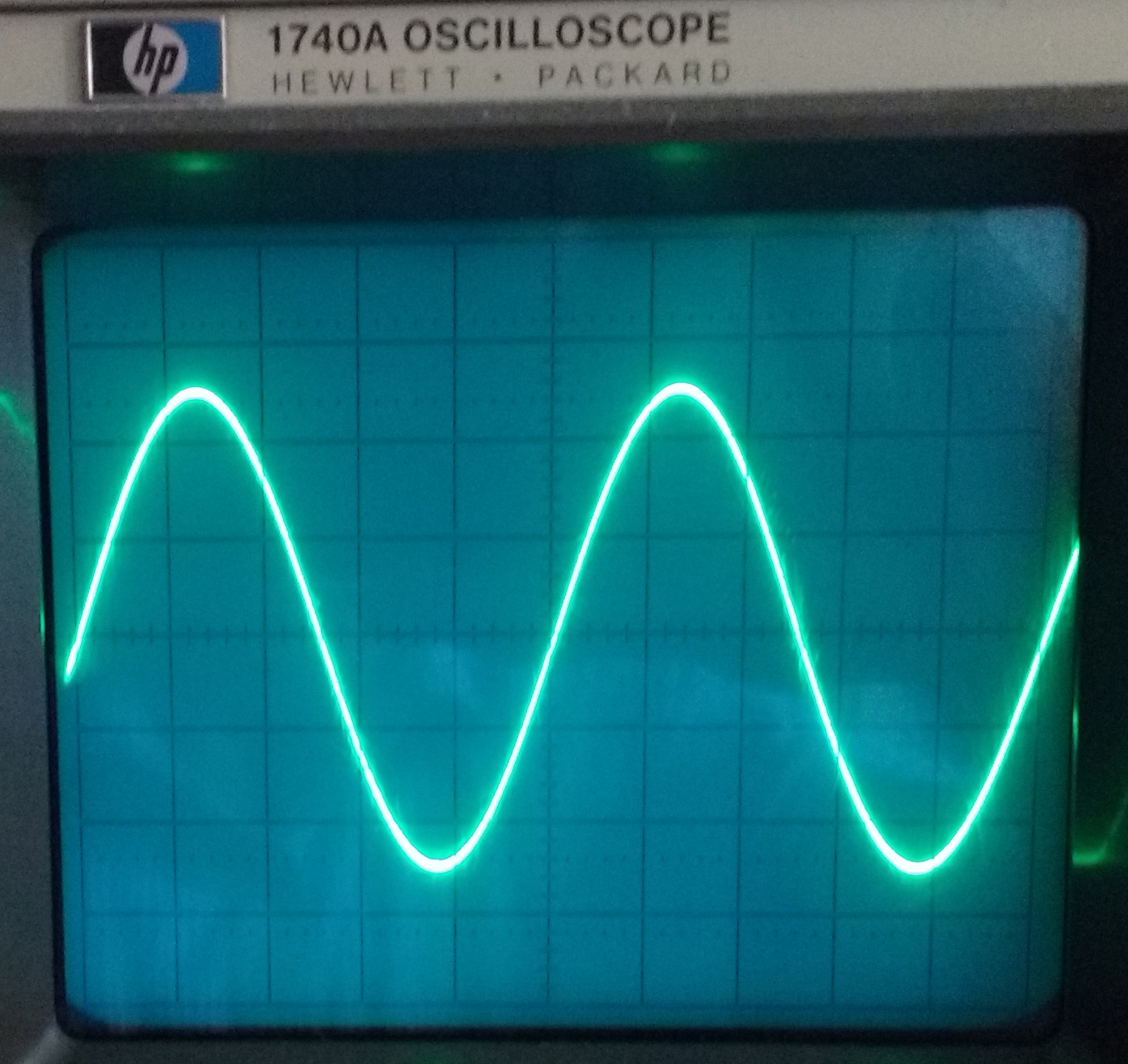
In most cases where 0, 90 degree signals are used in quadrature mixer drive, it is usual to be able to carefully adjust the amplitude of the signals to be identical. This is relatively easy using the two DDS cores. If one of the two DDS modules is producing a slightly different o/p amplitude this can be corrected. Keeping in mind the note above regarding use of matched oscilloscope probes, determine which of the two DDS core is producing the largest amplitude signal and for that module make the following simple modification. In the case of the DDS modules used by the author, there is a two pin link, labelled J3, this is the ground end of the 3k9 resistor which is used to set the o/p amplitude of the DDS signal, the 3k9 connects to pin 12 of the AD9850.
Obtain a physically small 500 Ohm or similar variable resistor. Solder the wiper and one track-end pin across the DDS module PCB-side of the J3 connector and remove the link. Restart the modules and using the 500 Ohm adjust the o/p signal amplitudes to be the same, as shown in photograph 3, which is two 1MHz carriers adjusted to be equal amplitude ( and in phase ).
Photograph 3:
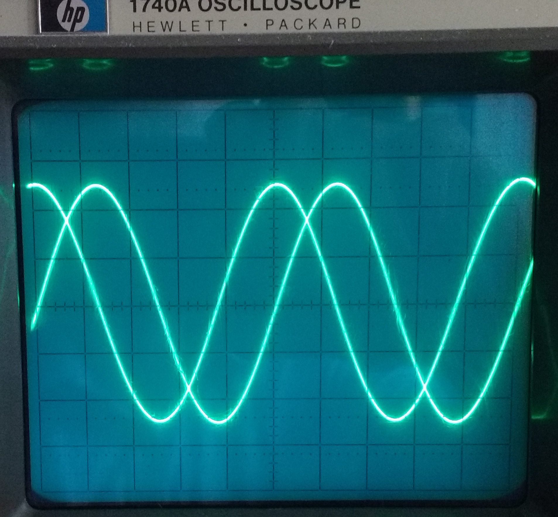
Two signals in quadrature
Photograph 4 shows two 1MHz carriers in quadrature.
Photograph 4:
Amplification
As the output signal of the non-amplified DDS core is not sufficient to drive a level 7 mixer, some form of amplification is often used. In the case of quadrature signals it is important that amplification of both signals is identical in amplitude and phase delay.
Notes for 16F876 28 pin version.
The required hardware circuit is essentially the minimum needed to run the device.
In addition to the usual Vcc and ground supplies, plus decoupling capacitors, add as below :
A crystal of 4 or 10MHz at the Osc1 and 2 pins, with 22pF each to ground.
A 100k Ohm pull up resistor on the !MCLR pin to Vcc.
Fit the standard MAX232 style serial interface device to port pins C6 and C7
Load hex code using your usual method.
In both the 4 and 10MHz hex versions the serial port uses 9600,8,none,1,none
i.e. 8 data bits, no parity, 1 stop bit, no flow control.